CMOS-Compatible Processing and Room Temperature Characterization for Scalable Quantum Computing beyond 2D Architectures
2025-04-29 09:15
2796 浏览
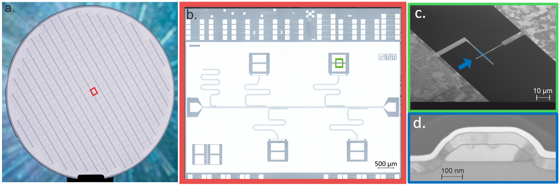
We report on an industry-grade CMOS-compatible qubit fabrication approach using a CMOS
pilot line, enabling a yield of functional devices reaching 92.8%, with a resistance spread evalu
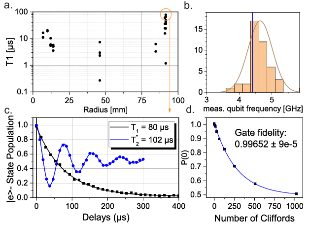
ated across the full wafer 200mm diameter of 12.4% and relaxation times (T1) approaching 80µs.
Furthermore, we conducted a comprehensive analysis of wafer-scale room temperature (RT) char
acteristics collected from multiple wafers and fabrication runs, focusing on RT measurements and
their correlation to low temperature qubit parameters. From defined test structures, a across-wafer
junction area variation of 10.1% and oxide barrier variation of 7.2% was calculated. Additionally,
we notably show a close-correlation between qubit junction resistance and frequency in accordance
with the Ambegaokar-Baratoff relation with a critical temperature Tc ∼ 0.71K. This overarching
relation sets the stage for pre-cooldown qubit evaluation and sorting. In particular, such early-on
device characterization and validation are crucial for increasing the fabrication yield and qubit fre
quency targeting, which currently represent major scaling challenges. Furthermore, it enables the
fabrication of large multichip quantum systems in the future. Our findings highlight the great poten
tial of CMOS-compatible industry-style fabrication of superconducting qubits for scalable quantum
computing in a foundry pilot line cleanroom.
Link to the article is here.