Wafer-Scale Characterization of Al/AlxOy/Al Josephson Junctions at Room Temperature
2025-04-25 17:24
2304 浏览arXiv:2504.16686
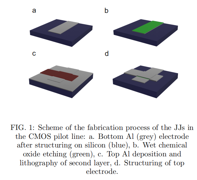
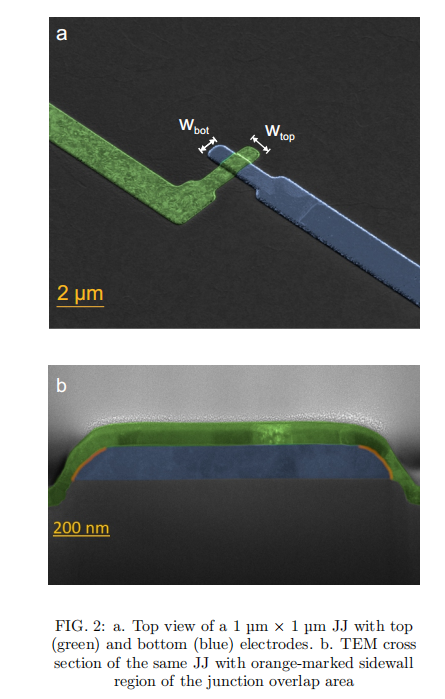
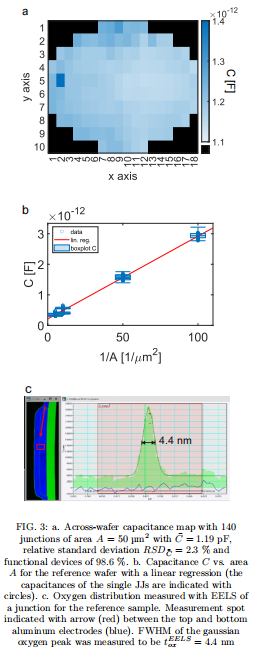
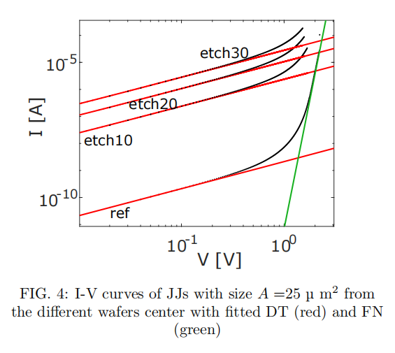
Josephson junctions (JJs) are the key element of many devices operating at cryogenic temperatures. Development of time-efficient wafer-scale JJ characterization for process optimization and control of JJ fabrication is essential. Such statistical characterization has to rely on room temperature techniques since cryogenic measurements typically used for JJs are too time consuming and unsuitable for wafer-scale characterization. In this work, we show that from room temperature capacitance and current-voltage measurements, with proper data analysis, we can independently obtain useful parameters of the JJs on wafer-scale, like oxide thickness, tunnel coefficient, and interfacial defect densities. Moreover, based on detailed analysis of current vs voltage characteristics, different charge transport mechanisms across the junctions can be distinguished. We exemplary demonstrate the worth of these methods by studying junctions fabricated on 200 mm wafers with an industrially scale-able concept based on subtractive processing using only CMOS compatible tools. From these studies, we find that our subtractive fabrication approach yields junctions with quite homogeneous average oxide thickness across the full wafers, with a spread of less then 3%. The analysis also revealed a variation of the tunnel coefficient with oxide thickness, pointing to a stoichiometry gradient across the junctions' oxide width. Moreover, we estimated relatively low interfacial defect densities in the range of 70 - 5000defects/cm2 for our junctions and established that the density increased with decreasing oxide thickness, indicating that the wet etching process applied in the JJs fabrication for oxide thickness control leads to formation of interfacial trap state.
